The Asus P2B-DS Rev 1.06 D03 clock generator chip is an ICS 9250CF-08, capable of generating up to 150Mhz FSB. However, for reasons unknown, Asus crippled the chip by only installing 3 FSB jumper headers on the P2B-DS Rev 1.06 D03 mainboards. As a result, the mainboard cannot be jumpered for FSB speeds over 133Mhz, and the available 133Mhz setting overclocks the PCI bus to 44.33Mhz (FSB/3).
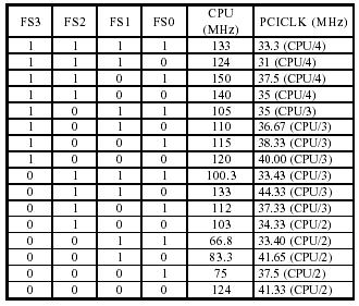
The table above shows the full range of FSB speeds supported by the ICS 9250CF-08 clock generator. Since Asus omitted the FS3 jumper, half these settings are unavailable - only the lower half of the table, where FS3 = 0, can be used. In order to enable the remaining settings, we must add the FS3 jumper header and a 10K ohm programming resistor. Unlike the P2B-S Rev 1.04. mainboards, which have unpopulated locations for the missing parts, the P2B-DS mainboards do not so we must improvise.
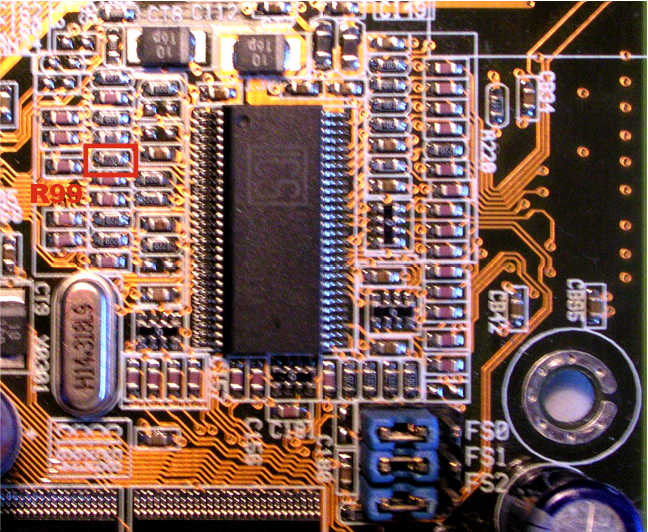
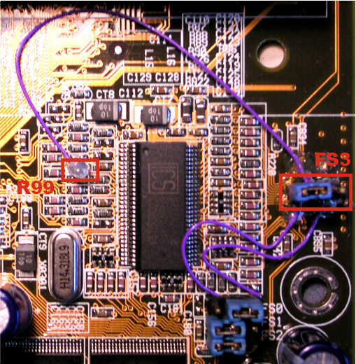
The 10K ohm programming resistor for FS3 header must be connected to the right hand side of R99. R99 is the 22 ohm terminating resistor for PCICLK0, and is connected to pin 9 of the ICS 9250CF-08 clock generator. Pin 9 is also the FS3 input to the clock generator.
FS3 In Progress
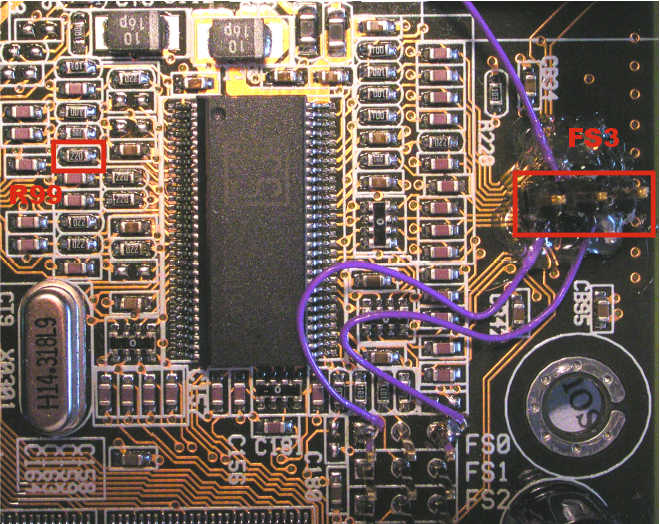
The FS3 jumper header is installed on a nearby vacant area, using hot-melt glue. The plastic base under the FSB headers is removed by pulling it up over the header pins. FS3 pin 1 is connected to FS0 pin 1, and FS3 pin 3 is connected to FS0 pin 3 with 30 gauge wire-wrap wire.
FS3 Installed
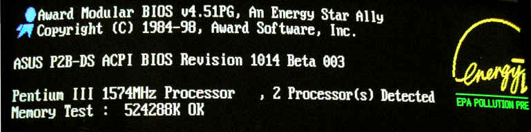
The modified P2B-DS Rev 1.06 D03 was tested with a pair of
PIII 450Mhz Slot 1 CPUs, running at 558Mhz (124Mhz FSB), and a 256MB
PC133 RAM module. Testing showed that the full range of FSB settings
supported by the ICS 9250CF-08 are now available, and that the
mainboard is stable at 124Mhz FSB.
The test CPUs ran for 5 minutes at 600Mhz (133Mhz FSB) before freezing,
but would not post at 140 or 150 Mhz FSB - faster CPUs will be needed
before the full capabilities of the modified P2B-DS Rev 1.06 D03 can be
tested.
Update: As it turns out, further mainboard modifications were made
in the course of our testing. Details here
and here.
Last updated May 4th, 2003 by p2b@sympatico.ca